The Story
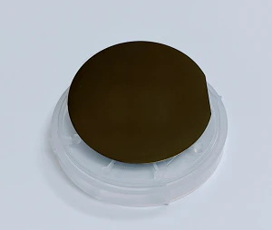
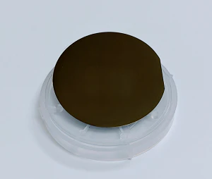
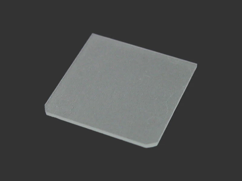
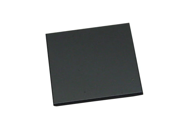
GaN Template on silicon is made by a hydride vapor phase epitaxy (HVPE)-based method. During the HVPE process, HCl reacts with molten Ga to form GaCl, which in turn reacts with NH3 to form GaN. GaN template on silicon is a cost effective way to replace GaN single crystal substrate.
- Research Grade , about 90 % useful area
-
Nominal GaN thickness: 0.5μm ± 0.1 μm
-
Front Surface finish (Ga-face): <1nm RMS, As-grown
-
Back surface finish: as received
-
GaN orientation: C-plane (00.1)
-
Polarity: Ga-face
-
Conduction Type: Undoped (N-)
-
Macro Defect Density: <5/cm^2
- Wafer base: Silicon [111], N type, P doped, Res: 1-10 ohm-cm, 2" diameter x 0.5mm, one side polished
- There is ~200nm AlN buffer layer between the silicon and GaN
Related data
- Please click here to see XRD Rocking curve of GaN template
- Please click here to see Dislocation vs Thickness of GaN template
Related Products
 |
|
|
|
|
|
|
Thin Films A-Z |
Crystal wafer A-Z |
Plasma Cleaner |
Wafer Containers |
Dicing saw |
Film Coater |


Description
GaN Template on silicon is made by a hydride vapor phase epitaxy (HVPE)-based method. During the HVPE process, HCl reacts with molten Ga to form GaCl, which in turn reacts with NH3 to form GaN. GaN template on silicon is a cost effective way to replace GaN single crystal substrate.
- Research Grade , about 90 % useful area
-
Nominal GaN thickness: 0.5μm ± 0.1 μm
-
Front Surface finish (Ga-face): <1nm RMS, As-grown
-
Back surface finish: as received
-
GaN orientation: C-plane (00.1)
-
Polarity: Ga-face
-
Conduction Type: Undoped (N-)
-
Macro Defect Density: <5/cm^2
- Wafer base: Silicon [111], N type, P doped, Res: 1-10 ohm-cm, 2" diameter x 0.5mm, one side polished
- There is ~200nm AlN buffer layer between the silicon and GaN
Related data
- Please click here to see XRD Rocking curve of GaN template
- Please click here to see Dislocation vs Thickness of GaN template
Related Products
|
|
|
|
|
|
|
Thin Films A-Z |
Crystal wafer A-Z |
Plasma Cleaner |
Wafer Containers |
Dicing saw |
Film Coater |