$567.00
Original: $1,620.00
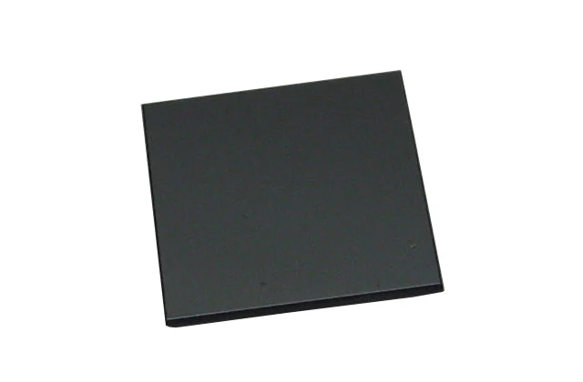
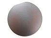
-65%InSb (111)- A 2" dia x 0.5 mm, Te-doped, N type, 1 side polished—
$1,620.00
$567.00The Story
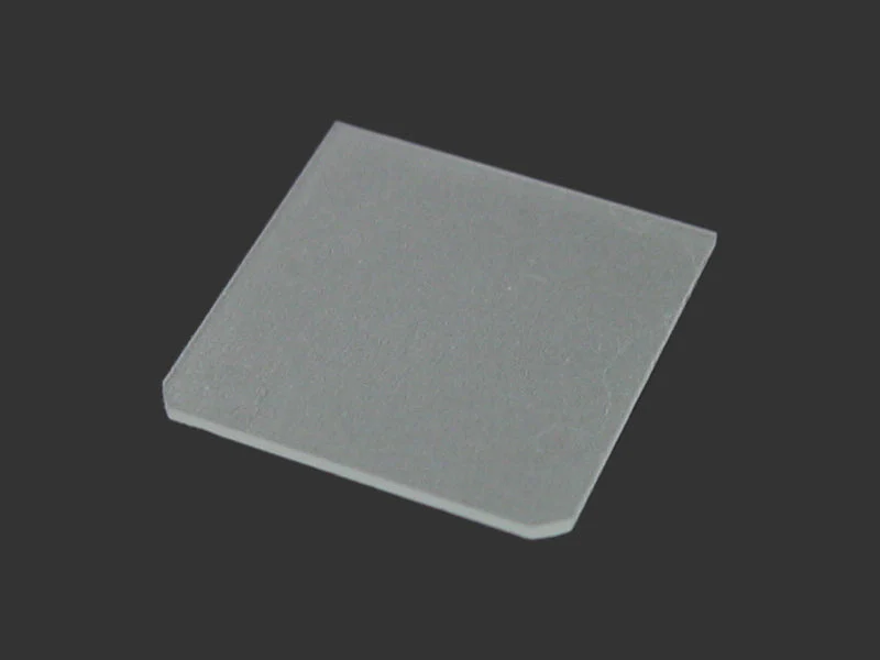
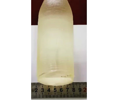
2" InSb wafer (N type, Te-doped)
- Size: 2" dia x 0.5mm thick with thickness tolerance +/- 25 um
- Orientation <111>A +/-0.5o with two reference flats
- Polishing: one-side polishd ( back side etched )
- Packing: Sealed under nitrogen with single wafer comtainer in 1000 class clean room
Properties
- Growth method CZ
- Orientation (111) A +/- 0.5o
- Orientation Flat <0-1-1> .<0-11>
- Doping Te-doped
- Conductivity type N type
- Resistivity: (1.1-3.3) E-4 ohm.cm
- Carrier Concentration (1.0E14 - 1.0 E15) cm-3
- Mobility >E5 cm2/Vs
- EPD < 1 E3 / cm -2
Description
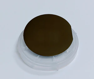
2" InSb wafer (N type, Te-doped)
- Size: 2" dia x 0.5mm thick with thickness tolerance +/- 25 um
- Orientation <111>A +/-0.5o with two reference flats
- Polishing: one-side polishd ( back side etched )
- Packing: Sealed under nitrogen with single wafer comtainer in 1000 class clean room
Properties
- Growth method CZ
- Orientation (111) A +/- 0.5o
- Orientation Flat <0-1-1> .<0-11>
- Doping Te-doped
- Conductivity type N type
- Resistivity: (1.1-3.3) E-4 ohm.cm
- Carrier Concentration (1.0E14 - 1.0 E15) cm-3
- Mobility >E5 cm2/Vs
- EPD < 1 E3 / cm -2