Original: $24.95
-65%$24.95
$8.73The Story
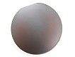
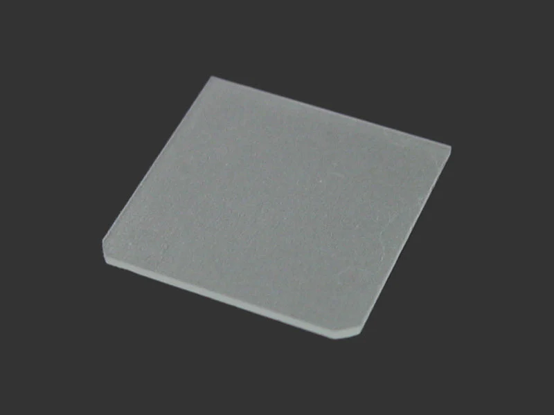
Device Layer | ||
Size: |
|
10x10 |
Type/Dopant: |
|
N type/P-doped |
Orientation: |
|
<1-0-0>+/-0.5 degree |
Thickness: |
|
2.5±0.5µm |
Resistivity: |
|
1-4 ohm-cm |
Finish: |
Front Side Polished |
|
|
Buried Thermal Oxide: | ||
Thickness: |
|
1.0 um +/- 0.1 um |
|
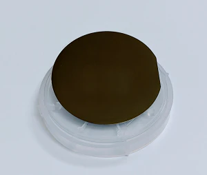
Handle Wafers: | ||
Type/Dopant |
P type/B-doped |
|
Orientation |
|
<1-0-0>+/-0.5 degree |
Resistivity: |
10-20 ohm.cm |
|
Thickness: |
|
625 +/- 15 um |
Finish: |
|
As received (not polished) |
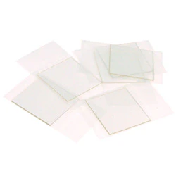
Related Products
 |
|
|
|
|
|
Thin Films A-Z |
Crystal wafer A-Z |
Plasma Cleaner |
Wafer Containers |
Dicing saw |
Film Coater |
Description
Device Layer | ||
Size: |
|
10x10 |
Type/Dopant: |
|
N type/P-doped |
Orientation: |
|
<1-0-0>+/-0.5 degree |
Thickness: |
|
2.5±0.5µm |
Resistivity: |
|
1-4 ohm-cm |
Finish: |
Front Side Polished |
|
|
Buried Thermal Oxide: | ||
Thickness: |
|
1.0 um +/- 0.1 um |
|
Handle Wafers: | ||
Type/Dopant |
P type/B-doped |
|
Orientation |
|
<1-0-0>+/-0.5 degree |
Resistivity: |
10-20 ohm.cm |
|
Thickness: |
|
625 +/- 15 um |
Finish: |
|
As received (not polished) |
Related Products
|
|
|
|
|
|
Thin Films A-Z |
Crystal wafer A-Z |
Plasma Cleaner |
Wafer Containers |
Dicing saw |
Film Coater |